Infineon Technologies GS66516B 650V GaN Bottom-side Cooled Transistor
Infineon Technologies GS66516B 650V GaN power transistor is designed for very low junction-to-case thermal resistance for demanding high power applications. The GS66516B is offered in a low inductance, low thermal resistance GaNPX™ package with a bottom-side cooled configuration. GaN on silicon power transistors allows for high current, high voltage breakdown, and high switching frequency.The high-current die performance and yield of the GS66516B are accomplished through patented Island Technology® cell layout. The GS66516B features reverse current capability, zero reverse recovery loss, and source sense for optimal high-speed design. Applications include onboard battery chargers, 400V DC/DC converters, inverters, UPS/industrial motor drives, fast battery charging, solar/wind power, and more.
Features
- 650V E-HEMT
- Low inductance GaNPX™ packaging
- 60A current IDS(max)
- 25mΩ Rds(on)
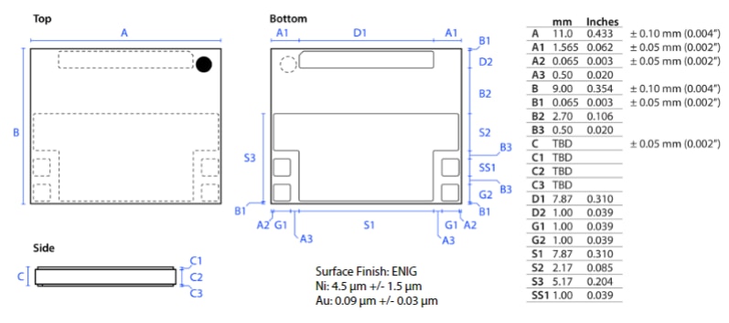
- Small 11mm x 9mm PCB footprint
- Bottom-side cooled
- Zero reverse recovery loss
- Reverse current capability
- Fast and controllable fall and rise times
- Dual gate and source sense pads for optimal board layout
- Ultra-low FOM Island Technology® die
Applications
- High-efficiency power conversion
- High-density power conversion
- AC-DC converters
- Bridgeless totem pole PFC
- ZVS Phase shifted full bridge
- Half Bridge topologies
- Synchronous buck or boost
- Uninterruptable power supplies
- Industrial motor drives
- Single and 3Φ inverter legs
- Solar and wind power
- Fast battery charging
- DC-DC converters
- On-Board battery chargers
- Traction drive
Additional Resource
GS66516B Dimensions

Publicado: 2017-05-17
| Actualizado: 2023-03-06


