Toshiba TCK40xG Load Switch ICs
Toshiba TCK40xG Load Switch ICs are 28V high input voltage external FET driver ICs. The TCK40xG ICs offer a slew rate control driver within a small WCSP6E package. These TCK40xG load switch ICs block reverse currents when the switch is turned off using external series FETs. The TCK40xG ICs feature an auto output discharge terminal, charge pump circuit, and inrush current reducing circuit. These load switch ICs operate within a -0.3V to 40V input voltage range and a -40°C to +85°C operating temperature range. The Toshiba TCK40xG Load Switch ICs are suitable for power management selector applications such as battery charging.Features
- 40V maximum input voltage
- Wide 2.7V to 28V input voltage operation range
- Auto output discharge terminal
- Charge pump circuit
- Inrush current reducing circuit
- Reverse current protection by external back-to-back MOSFETs
Specifications
- -0.3V to 40V maximum input voltage range
- 38µA typical output current
- 21kΩ typical DIS resistance
- 600kΩ typical control pull-down resistance
- 800mW power dissipation
- 28V over-voltage lockout
- 2.7V under-voltage lockout
- Temperature ranges
- -40°C to +85°C operating
- -55°C to +150°C storage
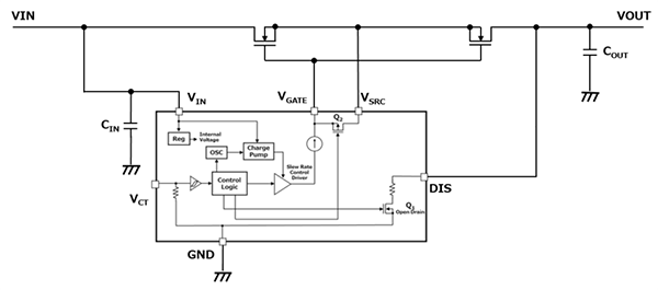
Typical Application

Block Diagram

Publicado: 2018-04-06
| Actualizado: 2023-02-02


