


Texas Instruments MSPM0G350x/MSPM0G350x-Q1 Mixed-Signal MCUs
Texas Instruments MSPM0G350x/MSPM0G350x-Q1 Mixed-Signal MCUs with CAN-FD Interface are part of the MSP highly integrated, ultra-low-power 32-bit MCU family. These MSPM0G350x/MSPM0G350x-Q1 are based on the enhanced Arm® Cortex®-M0+ 32-bit core platform operating at up to 80MHz frequency. The MCUs offer up to 128KB embedded flash program memory with built-in Error Correction Code (ECC) and up to 32KB SRAM with hardware parity option. These MCUs provide intelligent digital peripherals such as five general-purpose timers, 16-bit advanced control timers, two windowed watchdog timers, and one RTC with alarm and calendar modes. The TI MSPM0G350x/MSPM0G350x-Q1 MCUs provide data integrity and encryption peripherals (AES, CRC, and TRNG) and improved communication interfaces (four UART, two I2C, two SPI, and CAN 2.0/FD).
These MCUs support an extended temperature range of -40°C to 125°C and operate with supply voltages ranging from 1.62V to 3.6V. The MSPM0G350x-Q1 devices are AEC-Q100 qualified for automotive applications.
Features
- Core
- Arm 32-bit Cortex-M0+ CPU with memory protection unit, frequency up to 80MHz
- Operating characteristics
- Extended temperature of -40°C up to 125°C
- Wide supply voltage range of 1.62V to 3.6V
- Memories
- Up to 128KB of flash memory with error correction code (ECC)
- Up to 32KB of SRAM with hardware parity
- High-performance analog peripherals
- Two simultaneous sampling 12-bit 4Msps analog-to-digital converters (ADCs) with up to 17 external channels
- 14-bit effective resolution at 250ksps with hardware averaging
- One 12-bit 1MSPS digital-to-analog converter with integrated output buffer (DAC)
- Two zero-drift zero-crossover chopper op-amps (OPA)
- 0.5µV/°C drift with chopping
- Integrated programmable gain stage, up to 32x
- One general-purpose amplifier (GPAMP)
- Three high-speed comparators (COMP) with 8-bit reference DACs
- 32ns propagation delay in high-speed mode
- Support low-power mode operation down to 0.7µA
- Programmable analog connections between ADC, OPAs, COMP, and DAC
- Configurable 1.4V or 2.5V internal shared voltage reference (VREF)
- Integrated temperature sensor
- Integrated supply monitor
- Two simultaneous sampling 12-bit 4Msps analog-to-digital converters (ADCs) with up to 17 external channels
- Intelligent digital peripherals
- 7-channel DMA controller
- Math accelerator supports DIV, SQRT, MAC, and TRIG computations
- Seven timers support up to 22PWM channels
- One 16-bit general-purpose timer
- One 16-bit general-purpose timer supports QEI
- Two 16-bit general-purpose timers support low-power operation in STANDBY mode
- One 32-bit high-resolution general-purpose timer
- Two 16-bit advanced timers with deadband support up to 12PWM channels
- Two window-watchdog timers
- RTC with alarm and calendar mode
- Optimized low-power modes
- RUN: 96µA/MHz (CoreMark)
- SLEEP: 467µA at 4MHz
- STOP: 46µA at 32kHz
- STANDBY: 1.5µA with RTC and SRAM retention
- SHUTDOWN: 80nA with IO wake-up capability
- Enhanced communication interfaces
- Four UART interfaces; one supports LIN, IrDA, DALI, Smart Card, Manchester, and three support low-power operation in STANDBY mode
- Two I2C interfaces support up to FM+ (1Mbit/s), SMBus/PMBus, and wake-up from STOP mode
- Two SPIs, one SPI supports up to 32Mbits/s
- One Controller Area Network (CAN) interface supports CAN 2.0A or B and CAN-FD
- Clock system
- Internal 4MHz to 32MHz oscillator with up to ±1.2% accuracy (SYSOSC)
- Phase-locked loop (PLL) up to 80MHz
- Internal 32kHz low-frequency oscillator (LFOSC) with ±3% accuracy
- External 4MHz to 48MHz crystal oscillator (HFXT)
- External 32kHz crystal oscillator (LFXT)
- External clock input
- Data integrity and encryption
- Cyclic redundancy checker (CRC-16, CRC-32)
- True random number generator (TRNG)
- AES encryption with 128 or 256-bit key
- Flexible I/O features
- Up to 60GPIOs
- Two 5V tolerant IOs
- Two high-drive IOs with 20-mA drive strength
- Up to 60GPIOs
- Development support
- 2-pin serial wire debug (SWD)
- Package options
- 64-pin LQFP
- 48-pin LQFP, VQFN
- 32-pin VQFN
- 28-pin VSSOP
- Family members
- MSPM0G3505: 32KB Flash, 16KB RAM
- MSPM0G3506: 64KB Flash, 32KB RAM
- MSPM0G3507: 128KB Flash, 32KB RAM
Applications
- Motor control
- Home appliances
- Uninterruptible power supplies and inverters
- Electronic point-of-sale systems
- Medical and healthcare
- Test and measurement
- Factory automation and control
- Industrial transport
- Grid infrastructure
- Smart metering
- Communication modules
- Lighting
Datasheets
Videos
Functional Block Diagram

Development Tools
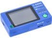
Texas Instruments C-GANG Low-Cost Gang Programmer
Gang programmer can program up to six targets at once & is compatible with the MSPM0/MSP430 devices.

Texas Instruments LP-MSPM0G3507 LaunchPad™ Development Kit
Facilitates the evaluation of the MSPM0G3507 M0+ MCU.
Publicado: 2023-12-28
| Actualizado: 2025-06-23