Renesas Electronics RL78/G1D BLUETOOTH® Low Energy MCUs
Renesas Electronics RL78/G1D BLUETOOTH® Low Energy MCUs offer a low level of current consumption at 4.3mA RF transmission current (0dBm output) and 3.5mA RF receiving current. The RL78/G1D provides built in circuit elements reducing cost and simplifying circuit design for the antenna connection by eliminating external parts. The user software is more efficient with a software stack that updates wirelessly.The Renesas RL78/G1D BLE MCUs contains the RL78/G1D, a 32MHz crystal resonator for RF chip, and an antenna, all in a compact (8.95 x 13.35 x 1.7mm) module. The functional pins of the RL78/G1D can be used for modem configuration or also for leveraging the strengths of the microcontroller for embedded configuration.
The RL78/G1D MCUs have an operating temperature of -25°C to 75°C and has has obtained Radio Law (Japan, FCC, IC, and CE) and Bluetooth SIG certification.
Features
- Low Power Technology (3.0V / MCU part: STOP)
- RF transmitter active: 4.3mA (TYP.)
- RF receiver active: 3.5mA (TYP.)
- RF sleep (POWER_DOWN mode) operation: 0.3μA (TYP.)
- On-Chip RF Transceiver
- Bluetooth v4.2 Specification (Low Energy Single mode)
- 2.4GHz ISM Band, GFSK modulation, TDMA/TDD Frequency Hopping (included AES encryption circuit)
- Adaptivity, exclusively for use in operation as a slave device
- Single ended RF interface
- 16-bit RL78-S2 CPU Core
- CISC Architecture (Harvard) with 3-stage pipeline
- Minimum instruction execution time: Can be changed from high speed (0.03125μs: @ 32MHz operation with high-speed on-chip oscillator) to ultra-low speed (30.5μs: @ 32.768kHz operation with subsystem clock)
- Multiply Signed & Unsigned: 16 x 16 to 32-bit result in 1 clock cycle
- 1-wire on-chip debug function
- Main Flash Memory
- 128KB / 192KB / 256KB (Block size: 1KB)
- On-chip single voltage flash memory with protection from block erase/writing
- Self-programming with secure boot swap function and flash shield window function
- Data Flash Memory
- Data Flash with background operation
- Data flash size: 8 KB size (Erase block size: 1KB)
- Erase Cycles: 1 Million (typ.)
- Erase/programming voltage: 1.8V to 3.6V
- RAM
- 12KB / 16KB / 20KB size
- Supports operands or instructions
- Back-up retention in all modes
- On-chip Oscillator
- High accuracy on-chip Oscillator for MCU
- 15kHz low-speed on-chip oscillator for MCU
- 32.768kHz On-chip oscillator for the RF slow clock
- Data Memory Access (DMA) Controller
- Up to 4 fully programmable channels
- Transfer unit: 8- or 16-bit
- Multiple Communication Interfaces
- 2x Simplified I2C
- 2x CSI (7-, 8-bit)
- 2x UART (7-, 8-, 9-bit)
- I2C
- Supply voltage Management
- Low voltage detection (LVD) with 12 setting options (Notification to Interrupt and/or reset function)
- Power-on reset (POR) monitor/generator
- Extended-Function Timers
- Multi-function 16-bit timers: 8 channels
- Real-time clock (RTC): 1 channel (full calendar and alarm function with watch correction function)
- Interval Timer: 12-bit, 1 channel
- Watchdog timer: 1 channel (window function)
- Rich Analog
- 8/10-bit resolution A/D converter (VDD = 1.6 to 3.6 V)
- Analog input: 8 channels
- Internal voltage reference (1.45 V) and temperature sensor
- Safety Functions
- Comply with the IEC60730 and IEC61508 safety standards
- General Purpose I/O
- I/O port: 32 (N-ch open drain I/O [withstand voltage of 6V]: 2, N-ch open drain I/O [VDD withstand voltage]: 9
- Different potential interface support: Can connect to a 1.8/2.5V device
- Standby function
- MCU part: Low power consumption mode: HALT, STOP Power saving mode: SNOOZE
- RF part :Low power saving mode with 6 setting (min. 0.1μA)
- Operating Voltage / Operating Ambient Temperature
- 1.6V to 3.6V / –40 to +85°C
- Package Type and Pin Count
- 48-pin HWQFN (6mm × 6mm) (0.4mm pitch)
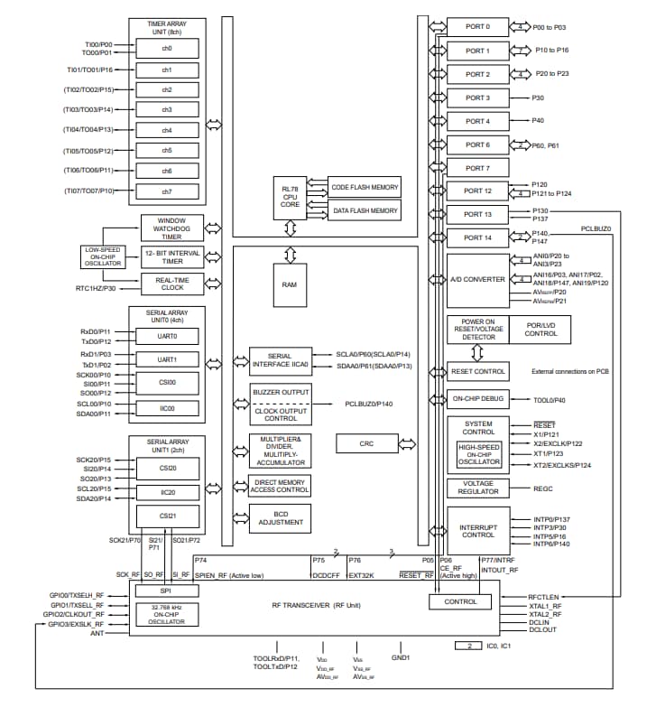
Block Diagram

Publicado: 2020-08-18
| Actualizado: 2025-11-04


